Loading...

Loading...
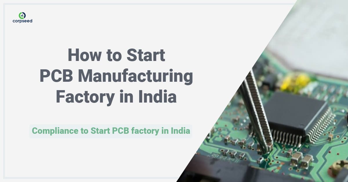
Printed circuit boards or better called PCBs are seen as an important component of the electronic items. This invention has found a place in almost all the electronics that work on computations which range from the simple calculators to other devices like that of the digital clocks.
About the Author

Vipan has more than 12 years of working experiences and guiding the team in the strategic Development and preparation of ESG reports. He is having a vast experiences of working in the field of Environment in legal, statutory, regulatory, environment compliance management and expertise in waste management. He is a Founder and MD of Corpseed. He is the one, who has developed World First Technology Driven AI Based Automated Compliance Model for All Businesses. He has worked with the Multinational Companies, such as Suncorp (Australian Bank), British Petroleum (UK), Eco- lab health care (USA), BHL, PGCL, UN-Group, SRY oil and gas, L&T, EVS electronics Ltd, Amzette, Faber, NTPC, Muthoot Finance, Capgemini etc.
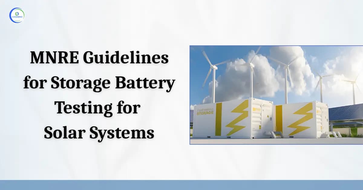
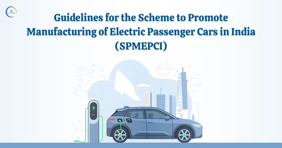
MNRE Guidelines for Storage Battery Testing for Solar Systems
2025-10-03
Top Articles
Most visited

Download Appointment Letter Format in Word and PDF
2022-02-17 • 156727 views
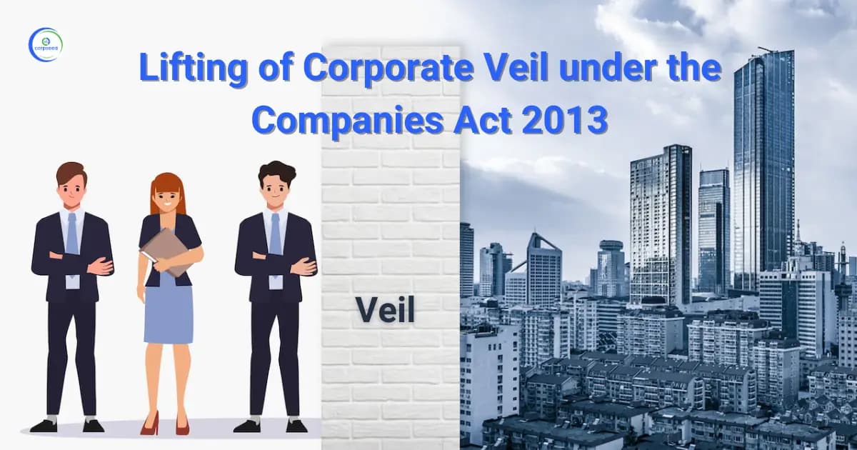
Lifting of Corporate Veil under the Companies Act 2013
2023-08-24 • 127634 views

Download Rental Agreement Format | Free Online Download Sample Format PDF, Word
2021-10-21 • 102699 views

Roles and Functions of Ngo in India
2021-12-08 • 53809 views
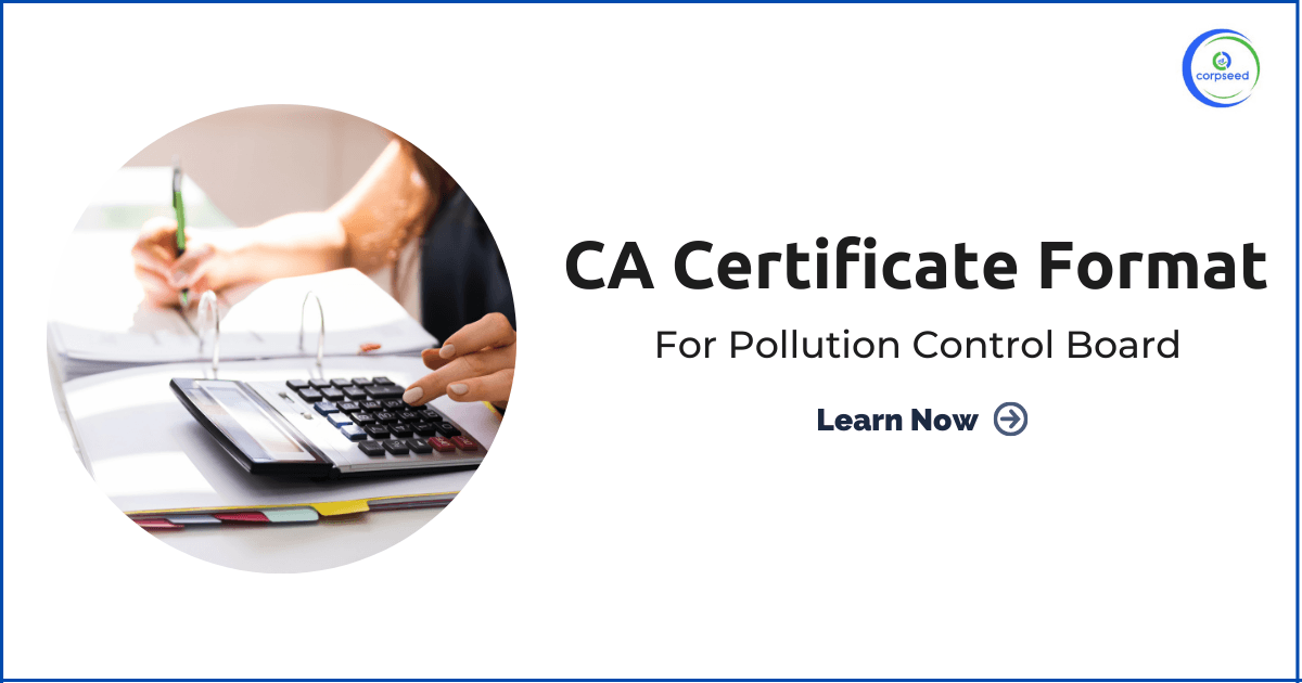
CA Certificate Format For Pollution Control Board
2022-06-22 • 48962 views
Latest Articles
Recently published
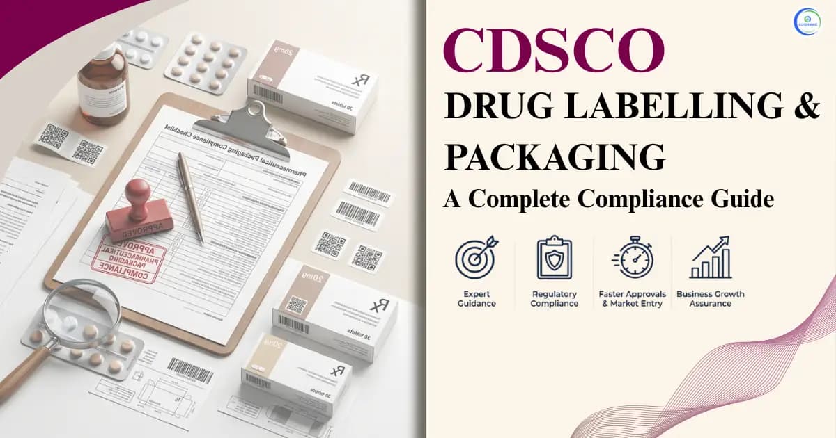
CDSCO Drug Labelling & Packaging: A Complete Compliance Guide
2026-06-24 • 2498 views
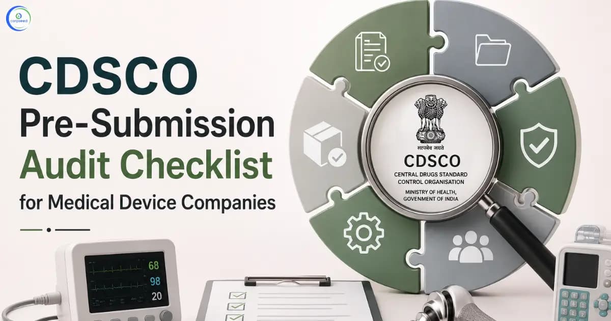
CDSCO Pre-Submission Audit Checklist for Medical Device Companies
2026-06-22 • 3929 views
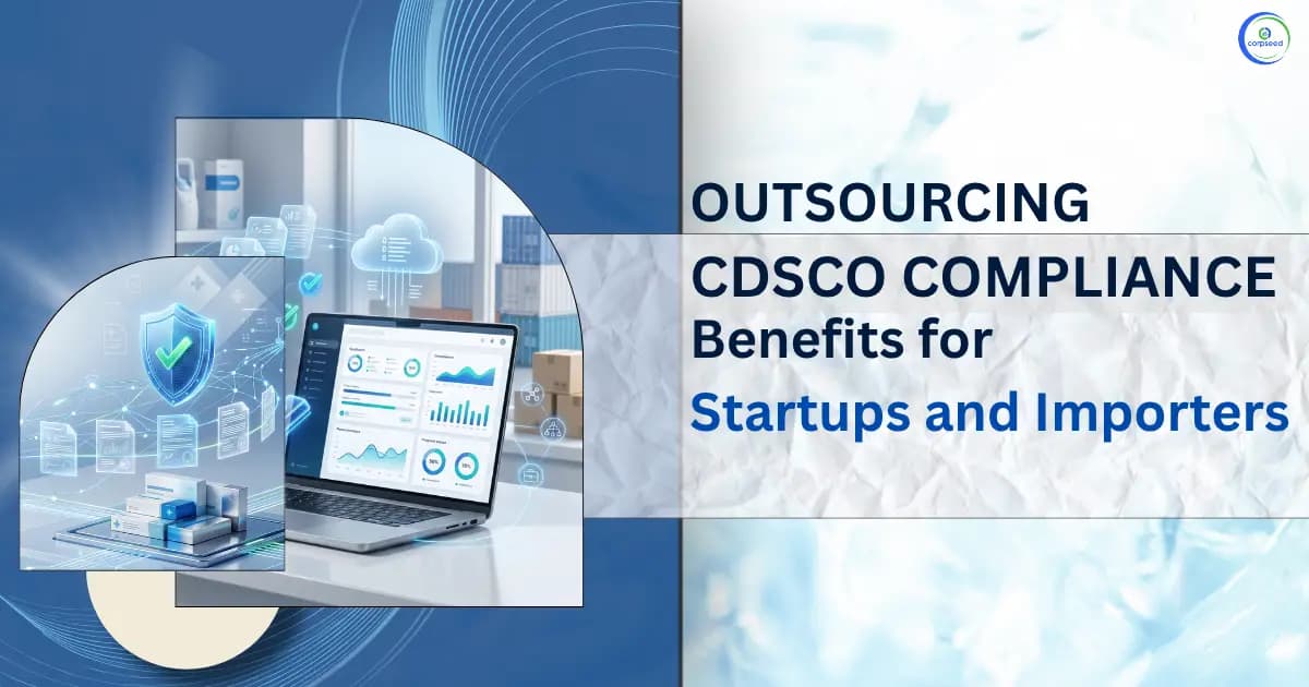
Outsourcing CDSCO Compliance: Benefits for Startups and Importers
2026-06-19 • 4408 views
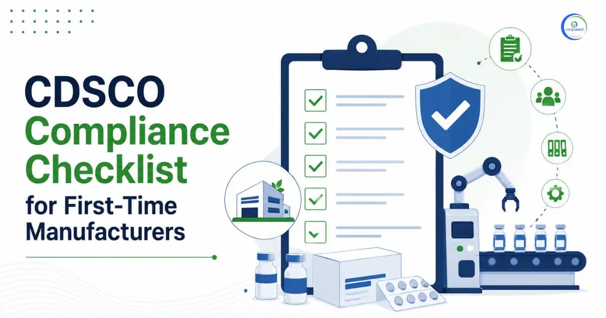
CDSCO Compliance Checklist for First-Time Manufacturers
2026-06-16 • 4794 views
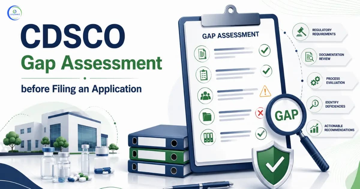
CDSCO Gap Assessment before Filing an Application
2026-06-15 • 4242 views
Top News
Trending
Salary Slip Format In Excel, Word, PDF, PaySlip Format Online
2023-02-27
.png&w=1536&q=75)
Increment Letter Format - Salary Increment Letter With Salary Break Up Format In Word and PDF
2023-02-27

Latest Marriage Biodata Formats | Biodata Format for Marriage Download in Word and PDF
2023-02-27
New Form 15G in Word Format | Download Form 15G in Word and PDF Format
2023-02-27
.png&w=1536&q=75)
Job Offer Letter Format With Word And PDF Templates Download
2022-07-19
Latest News
Fresh updates
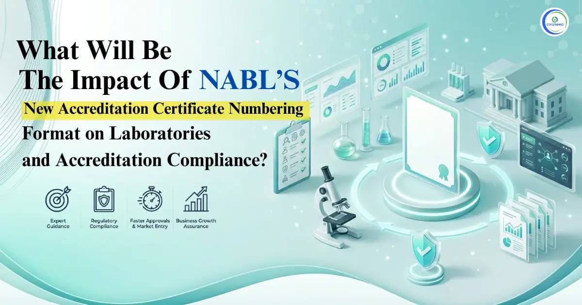
What Will Be the Impact of NABL's New Accreditation Certificate Numbering Format on Laboratories and Accreditation Compliance?
2026-06-24
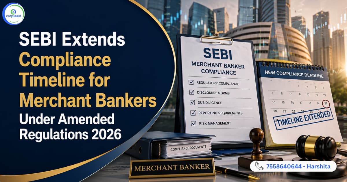
SEBI Extends Compliance Timeline for Merchant Bankers Under Amended Regulations 2026
2026-06-24
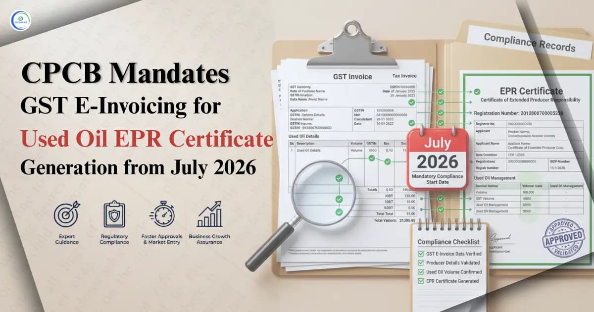
CPCB Mandates GST E-Invoicing for Used Oil EPR Certificate Generation from July 2026
2026-06-24
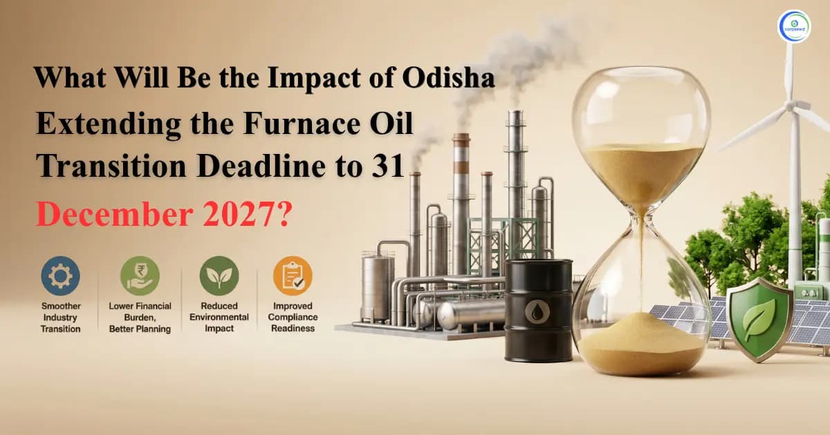
What Will Be the Impact of Odisha Extending the Furnace Oil Transition Deadline to 31 December 2027?
2026-06-19
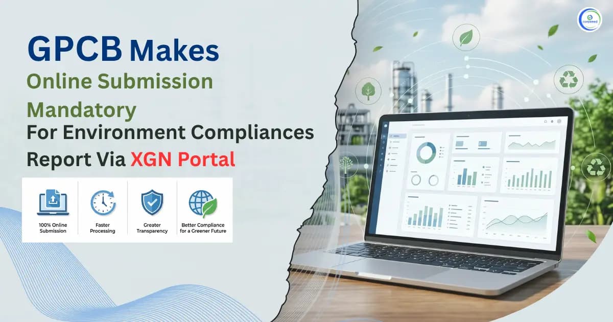
GPCB Makes Online Submission Mandatory for Environmental Compliance Reports via XGN Portal
2026-06-17